Figure
Description
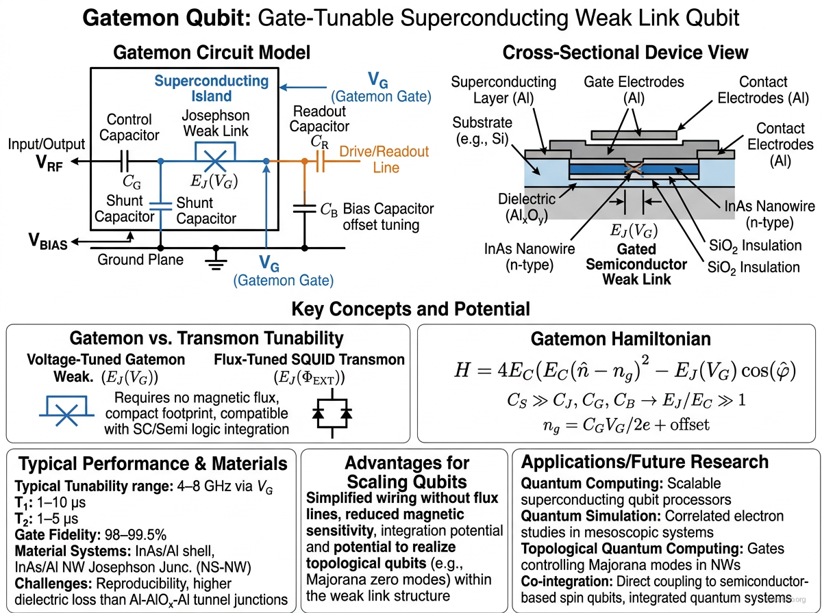
The gatemon is a superconducting transmon-style qubit where the conventional tunnel-barrier Josephson junction is replaced by a semiconductor nanowire (typically InAs or InAs/Al) with a gate-tunable weak link. The supercurrent through the nanowire depends on the gate voltage applied to the semiconductor channel, making — and therefore the qubit frequency — voltage-tunable rather than flux-tunable.
Introduced independently by Larsen et al. and de Lange et al. in 2015, the gatemon inherits the transmon’s charge-noise insensitivity () while gaining two advantages:
- Voltage tunability: no magnetic flux required, eliminating flux-noise sensitivity and simplifying wiring.
- Semiconductor integration: the nanowire channel can host exotic physics (Andreev bound states, Majorana modes) while simultaneously serving as the qubit element.
The current-phase relation of the semiconductor weak link can deviate from sinusoidal, introducing higher harmonics () that modify the anharmonicity and energy-level structure compared to a standard transmon.
The tradeoff is that semiconductor junctions currently have higher loss and lower reproducibility than aluminum oxide tunnel junctions, resulting in shorter coherence times than state-of-the-art transmons.
Hamiltonian
Same form as the transmon, but with gate-voltage-dependent Josephson energy:
The current-phase relation of the semiconductor weak link can deviate from sinusoidal, introducing higher harmonics:
which modifies the anharmonicity and energy-level structure compared to a standard transmon.
Motivation
- Flux-tunable transmons require magnetic flux bias lines that add wiring complexity and introduce flux noise.
- The gatemon replaces this with a DC gate voltage — simpler, lower noise, and compatible with semiconductor qubit co-integration on the same chip.
- Provides a platform for exploring novel semiconductor-superconductor physics (Andreev states, Majorana modes) within a circuit-QED-compatible architecture.
Experimental Status
First demonstrations — Larsen et al. and de Lange et al. (2015):
- Larsen et al. demonstrated the first gatemon using an InAs nanowire Josephson junction, showing gate-voltage tunability of the qubit frequency from 4–8 GHz.
- de Lange et al. independently demonstrated a gatemon with two-qubit coupling.
- Coherence times of –s, limited by semiconductor junction losses.
Ge/SiGe gatemon — Casparis et al. (2018):
- Extended the gatemon concept to a proximitized two-dimensional electron gas (2DEG) platform.
- Improved junction reproducibility compared to nanowire devices.
Ongoing development (2020s):
- Continued materials and fabrication improvements targeting higher coherence.
- Integration with Majorana-based topological qubit proposals.
Key Metrics
| Metric | Value | Notes | Fidelity reference |
|---|---|---|---|
| 1–10 μs | Limited by semiconductor junction loss | Larsen et al. 2015 | |
| 1–5 μs | Dominated by charge and junction noise | — | |
| Frequency tunability | 4–8 GHz | Via gate voltage | — |
| 1Q gate fidelity | 98–99.5% | Improving with materials | Larsen et al. 2015 |
| Operating temperature | 10–20 mK | Dilution refrigerator | — |
References
Original demonstrations
- T. W. Larsen et al., “Semiconductor-Nanowire-Based Superconducting Qubit,” Phys. Rev. Lett. 115, 127001 (2015)
2DEG gatemon
- L. Casparis et al., “Superconducting gatemon qubit based on a proximitized two-dimensional electron gas,” Nature Nanotech. 13, 915 (2018)
Linked Papers
Evergreen context
- josephson-junction-as-nonlinear-element — the gatemon keeps transmon physics but replaces the oxide tunnel barrier with a semiconductor weak link whose is tuned electrostatically.
- charge-noise-sweet-spot — its protection story is still the transmon one: large flattens charge sensitivity, while the gate adds a control knob without reverting to charge-qubit fragility.
- quantum-hardware — this is the cleanest bridge between mainstream superconducting control stacks and semiconductor-process ambitions.
Related Entries
- transmon — parent qubit architecture; gatemon replaces the tunnel junction
- gatemonium — related semiconductor-superconductor hybrid qubit
- andreev-spin-qubit — same material platform, spin degree of freedom