Figure
Description
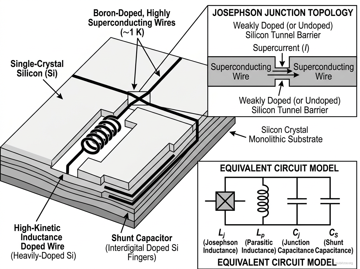
The all-semiconductor superconducting qubit is a proposed architecture in which every component of a superconducting quantum circuit — Josephson junctions, wires, inductors, capacitors — is fabricated within a single group-IV semiconductor crystal (Si or Ge) using precision atomic-scale doping. The heavily doped regions become superconducting at sub-kelvin to order-1 K temperatures, and the undoped or weakly doped crystal between them forms the tunnel barrier. No deposited metal is involved: superconductivity is meant to arise inside the doped semiconductor itself.
Conventional superconducting qubits use deposited metal films (Al, Nb, Ta) on a semiconductor or sapphire substrate. Even “hybrid” super-semi devices like the gatemon deposit a metal superconductor onto a semiconductor nanowire or 2DEG. The all-semiconductor approach eliminates the metal entirely:
- Superconducting regions: Created by dense substitutional doping (e.g., boron in Si at densities >10²¹ cm⁻³), which induces superconductivity via the BCS mechanism with – K.
- Josephson junctions: Formed at the boundary between a doped (superconducting) region and an undoped (insulating) region — a doped-undoped-doped structure within the same crystal.
- Wires and interconnects: Heavily doped superconducting channels patterned by STM hydrogen lithography or focused ion beam implantation.
- Capacitors: Doped plates separated by undoped semiconductor dielectric — all within one crystal.
The critical advantage is the elimination of metal-semiconductor interfaces and amorphous oxide tunnel barriers that often dominate loss budgets in conventional superconducting circuits. In the optimistic limit, most of the active electromagnetic energy would live inside a crystalline host rather than at dirty deposited-film interfaces. That does not make the device magically disorder-free: dopant inhomogeneity, barrier engineering, and acceptor-placement accuracy remain real materials challenges.
Atomic-precision placement of dopants using scanning tunneling microscope (STM) hydrogen desorption lithography enables deterministic positioning of individual dopant atoms. This technique, developed for silicon donor qubits (Kane qubit), can be repurposed to create superconducting circuits with atomic-scale control of junction dimensions and barrier thickness.
Hamiltonian
The circuit Hamiltonian is not exotic. It follows standard superconducting-qubit forms (transmon, fluxonium, etc.) depending on the chosen circuit, with the novelty residing in the junction and capacitor materials:
with determined by the doped-undoped-doped junction geometry, and from the crystalline capacitor. For the experimentally realized Si:B benchmark used in the 2014 proposal, implies , so the platform still lives firmly in the dilution-refrigerator regime.
Motivation
- Interface elimination: Removes all lossy metal-substrate, metal-air, and amorphous oxide interfaces — potentially a step change in coherence.
- CMOS-native: Built entirely within silicon/germanium — ultimate compatibility with semiconductor foundry processes.
- Monolithic integration: A Si crystal can host both superconducting circuits (doped regions) and spin qubits (donor atoms) in the same chip — true monolithic quantum processor.
- Defect-free barriers: Crystalline tunnel barriers instead of amorphous AlO could dramatically reduce two-level system (TLS) defect density.
- Atomic precision: STM lithography enables sub-nm control of junction dimensions.
Experimental Status
As of this 2026 audit, no peer-reviewed all-semiconductor superconducting Josephson junction, SQUID, or qubit realization was found that supersedes the 2014 proposal. The experimentally established pieces remain partial ingredients, not the full architecture:
- Hole-doped superconducting Si and Ge exist in laser-doped or implanted films, so the underlying superconducting materials claim is real.
- Atomic-precision STM lithography exists for donor-defined semiconductor nanostructures, but a corresponding acceptor-defined superconducting qubit flow has not been demonstrated.
- Closest adjacent qubit direction: the mergemon experimentally pursues the same interface-reduction intuition, but with conventional metal Josephson junctions rather than an all-semiconductor monolith.
Key Metrics
| Metric | Value | Notes | Fidelity reference |
|---|---|---|---|
| Demonstrated Si:B | 0.35–0.6 K | Homogeneous laser-doped Si:B films reached K; thinner or less-dense structures can be lower | Shim and Tahan 2014 |
| Optimistic projected | ~1.2 K | Proposal-level estimate for aggressively dense multilayer acceptor doping, not an experimental result | Shim and Tahan 2014 |
| Gap at K | eV | Direct BCS estimate quoted from the experimentally realized Si:B benchmark used in the paper | Shim and Tahan 2014 |
| Junction | ~0.14 mV (STJ), ~0.18 mV (weak link) | Zero-temperature estimates implied by the proposal’s and junction formulas | Shim and Tahan 2014 |
| Fabrication concept | STM H-lithography + acceptor doping | Atomically precise in principle, but still a proposal-stage qubit flow | Shim and Tahan 2014 |
Scaling Considerations
- Interface loss upside: The platform’s whole value proposition is cleaner participation, not exotic Hamiltonian physics.
- Validation gap: The superconducting materials and the atomically precise semiconductor patterning have each been shown separately, but not yet fused into a peer-reviewed monolithic qubit stack.
- Cryogenic margin: Even the optimistic superconducting transition temperatures remain in the same broad regime as aluminium-class circuit operation, so this is not a path to warm superconducting qubits.
- Serial fabrication bottleneck: STM lithography is still slow and bespoke relative to foundry transmon fabrication.
- Integration upside: If it ever works, one crystalline host for superconducting circuits, donor devices, and shared fabrication flows would be genuinely unusual.
References
Original proposal
- Y.-P. Shim and C. Tahan, “Bottom-up superconducting and Josephson junction devices inside a group-IV semiconductor,” Nat. Commun. 5, 4225 (2014) — arXiv:1309.0015
Related theory
- Y.-P. Shim and C. Tahan, “Semiconductor-inspired design principles for superconducting quantum computing,” Nat. Commun. 7, 11059 (2016) — arXiv:1507.07923
Adjacent experimental direction
- R. Zhao et al., “Merged-Element Transmon,” Phys. Rev. Applied 14, 064006 (2020) — arXiv:2003.02686
Linked Papers
Evergreen context
- josephson-junction-as-nonlinear-element — the proposal keeps standard Josephson-circuit physics, but tries to realize the nonlinear element entirely inside a doped single crystal instead of across deposited metal interfaces.
- quantum-hardware — its real significance is architectural: one semiconductor host for superconducting circuits, donor devices, and shared fabrication flows.
- divincenzo-criteria — this note is a useful reminder that elegant materials integration is not enough by itself; the missing evidence is still competitive initialization, control, readout, and coherence.
Related Entries
- mergemon — Merged-element transmon sharing the interface-elimination philosophy
- gatemon — Hybrid super-semi qubit with metal superconductor on semiconductor
- gatemonium — Gatemon variant with multiple junctions
- dual-rail-superconducting-qubit — Encoded superconducting qubit proposal explicitly framed as a good fit for variable super-semi junctions
- kane-qubit — Silicon donor qubit using same STM fabrication technique
- silicon-spin-qubit — Silicon platform cousin
- transmon — Conventional transmon that this aims to replace