Figure
Description
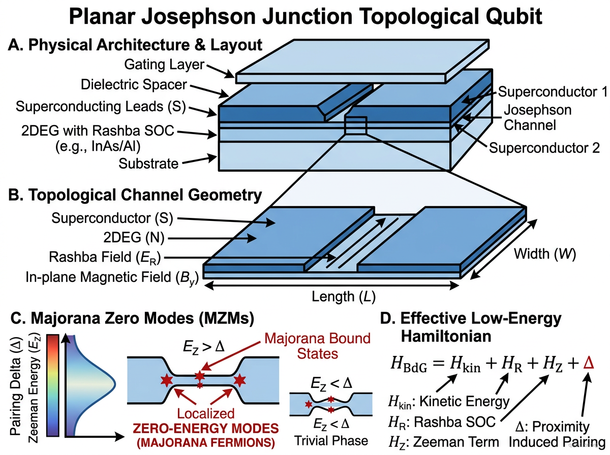
The planar Josephson junction (pJJ) topological qubit hosts Majorana zero modes at the ends of a topological superconducting channel formed in a two-dimensional electron gas (2DEG) sandwiched between two superconducting leads. Unlike nanowire-based approaches, the pJJ geometry uses a lithographically defined junction in a planar 2DEG — offering better scalability, easier fabrication, and less stringent magnetic field alignment requirements.
A 2DEG with strong Rashba spin-orbit coupling (typically InAs or InAs/Al heterostructures) is contacted by two superconducting leads separated by a narrow gap. When an in-plane Zeeman field is applied and the superconducting phase difference across the junction is tuned near , the 1D channel between the leads enters a topological superconducting phase. Majorana zero modes appear at the channel endpoints.
Key advantages over nanowires include planar geometry compatible with standard lithographic fabrication, relaxed magnetic field alignment requirements, phase control via SQUID-loop geometries, and diagnostic tools where the critical current shows a sharp minimum at the topological phase transition.
Fornieri et al. (2019) observed signatures of topological superconductivity in InAs 2DEG-Al planar Josephson junctions, including closing and reopening of the superconducting gap as a function of in-plane field. Ren et al. (2019) independently demonstrated similar signatures in epitaxial Al-InAs devices.
Hamiltonian
The Bogoliubov-de Gennes Hamiltonian for the junction region:
where is the Rashba coefficient, is the Zeeman energy, is the proximity-induced pairing (nonzero under the leads, zero in the junction), and , are Nambu and spin Pauli matrices. The topological phase transition occurs when:
at phase difference , with the topological gap .
Motivation
- Planar scalability: Fully compatible with standard semiconductor lithography — no nanowire growth or mechanical assembly.
- Phase tunability: The superconducting phase difference provides an additional tuning knob; at , topological protection is maximized.
- Relaxed field requirements: Does not require precise magnetic field alignment along a 1D wire axis.
- In-situ diagnostics: Critical current minimum at the topological transition provides a built-in probe of the topological phase.
- Network scalability: Multiple junctions can be patterned on a single 2DEG chip for braiding operations.
Evergreen context
- quantum-hardware frames the planar junction route as a hybrid of semiconductor fabrication and superconducting proximity physics, aiming for a more lithography-friendly topological stack.
- spin-orbit-coupling-for-qubit-control is central here, because Rashba coupling in the 2DEG is one of the ingredients that opens the topological gap when combined with phase bias and Zeeman splitting.
- divincenzo-criteria highlights the gap between observing topological-transition signatures and demonstrating a practical qubit with robust initialization, readout, and entangling control.
- josephson-junction-as-nonlinear-element provides adjacent circuit intuition: in this platform the junction is not mainly valued for anharmonicity, but for the superconducting phase bias that helps tune the topological channel.
Key Metrics
| Metric | Value | Notes | Fidelity reference |
|---|---|---|---|
| Topological gap | ~20–50 μeV | At optimal field/phase | Pientka et al. 2017 |
| Operating temperature | <100 mK | Dilution refrigerator | Fornieri et al. 2019 |
| Junction width | 50–150 nm | Lithographically defined | Fornieri et al. 2019 |
| Phase tunability | Full 0–2π | Via flux through SQUID loop | Pientka et al. 2017 |
Scaling Considerations
- Fabrication: Fully planar, compatible with semiconductor foundry processes.
- Networks: Multiple junctions can be patterned on a single 2DEG chip for braiding operations.
- Tetron geometry: Microsoft’s Majorana 1 processor uses related InAs/Al heterostructure physics in an H-shaped tetron layout.
- Phase control: SQUID-loop geometries allow electrical tuning of without external flux.
References
Original proposal
- F. Pientka et al., “Topological Superconductivity in a Planar Josephson Junction,” Phys. Rev. X 7, 021032 (2017) — arXiv:1609.09482
Experimental demonstrations
- A. Fornieri et al., “Evidence of topological superconductivity in planar Josephson junctions,” Nature 569, 89 (2019) — arXiv:1809.03037
Related theory
- A. Stern and E. Berg, “Topological Superconductivity in Planar Josephson Junctions,” Phys. Rev. Lett. 122, 107701 (2019)
Linked Papers
Related Entries
- majorana-topological-qubit — General Majorana qubit concept
- tetron-qubit — Microsoft’s tetron uses related InAs/Al heterostructure physics
- andreev-spin-qubit — Andreev bound states in related junction geometries
- gatemon — Semiconductor-superconductor hybrid using similar materials