Figure
Description
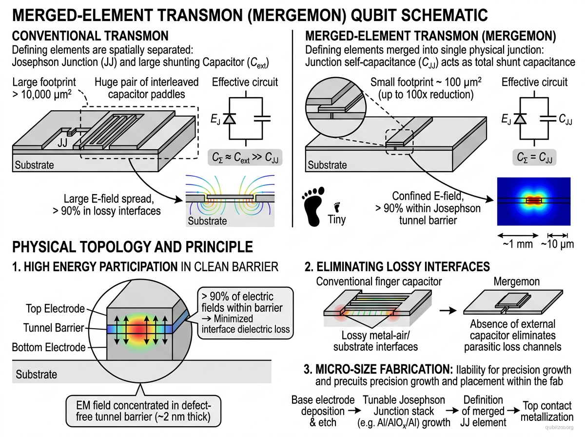
The merged-element transmon (mergemon or MET) is a superconducting qubit in which the Josephson junction’s intrinsic self-capacitance replaces the large external shunt capacitor of a conventional transmon. This merges the two defining circuit elements into one, shrinking the qubit footprint by ~100× and confining >90% of the electromagnetic energy to the tunnel barrier region — away from the lossy interfaces that limit coherence in standard transmons.
The mergemon concept traces to the proposal by Shim and Tahan (2014) to build superconducting devices inside a group-IV semiconductor using precision atomic-scale doping. The Pappas group (NIST/CU Boulder) demonstrated the first mergemon prototypes using Al/AlOₓ/Al overlap junctions (2020–2021): micrometer-scale junctions with long oxidation, achieving = 10–90 μs. The FinMET variant uses silicon fin-based merged transmons compatible with CMOS foundry processing. Ongoing work explores crystalline barriers (WSe₂ or epitaxial semiconductor barriers) aiming to eliminate amorphous dielectric loss entirely.
In a standard transmon, the shunt capacitor (typically ~100 fF, ~300 μm across) dominates the device area. Surface dielectric loss at the capacitor’s metal-substrate-vacuum interfaces is the primary coherence limiter. The mergemon eliminates this capacitor: the junction itself provides the required capacitance (20–100 fF for transmon operation), and the electric field is concentrated inside the junction barrier rather than at exposed surfaces.
Hamiltonian
Same as the transmon:
but with set by the junction self-capacitance rather than an external shunt: . The merged element enforces , concentrating field energy in the barrier.
Motivation
- 100× footprint reduction: Eliminates the large shunt capacitor, enabling dramatically denser qubit arrays.
- Interface loss elimination: Moves dominant loss mechanism from surface dielectrics (uncontrollable) to junction barrier quality (engineerable).
- CMOS compatibility: FinMET variant uses mature semiconductor fin-etch processes for foundry-scale manufacturing.
- Crystalline barrier frontier: All-crystalline mergemons could push coherence beyond the amorphous AlO limit.
- Super-semi integration: Natural platform for merging spin qubit and transmon functionality on a single chip.
Experimental Status
First mergemon demonstration — Zhao et al. (2020):
- Al/AlOₓ/Al overlap junction mergemon with ~100× footprint reduction
-
90% electromagnetic energy participation in the tunnel barrier
- Demonstrated transmon-regime operation without external shunt capacitor
Improved coherence — Madon et al. (2021):
- = 10–90 μs for standard overlap mergemons
- > 100 μs achieved with ABAA (anneal-based) annealing protocol
- Junction loss demonstrated to not be the dominant coherence limiter
Key Metrics
| Metric | Value | Notes | Fidelity reference |
|---|---|---|---|
| 10–90 μs | Al/AlOₓ overlap mergemon | Zhao et al. 2020 | |
| (annealed) | >100 μs | With ABAA annealing | — |
| Footprint reduction | ~100× | vs. standard transmon | Zhao et al. 2020 |
| Energy confinement | >90% in barrier | Reduced surface participation | Zhao et al. 2020 |
| Junction capacitance | 20–100 fF | Self-capacitance of large-area junction | — |
| CMOS compatibility | Yes | FinMET variant | — |
Scaling Considerations
- Density: ~100× smaller footprint enables dramatically denser qubit arrays.
- Loss mechanism shift: Moves dominant loss from surface dielectrics to junction barrier quality — a more controllable parameter.
- Fabrication: Compatible with semiconductor foundry processes (fin etch, trilayer deposition). Path to industrial-scale manufacturing.
- Materials frontier: Crystalline barriers (epitaxial semiconductors, 2D materials) may push coherence beyond amorphous AlOₓ limits.
- Super-semi integration: Natural platform for merging spin qubit and transmon functionality on a single chip.
References
Original concept
- Y.-P. Shim and C. Tahan, “Bottom-up superconducting and Josephson junction devices inside a group-IV semiconductor,” Nat. Commun. 5, 4225 (2014) — arXiv:1309.0015
Experimental demonstrations
- R. Zhao et al., “Merged-Element Transmon,” Phys. Rev. Applied 14, 064006 (2020) — arXiv:2003.02686
Linked Papers
Evergreen context
- josephson-junction-as-nonlinear-element — the merged-element idea makes the junction itself supply both anharmonicity and most of the capacitance
- charge-noise-sweet-spot — mergemon stays in the transmon logic of suppressing charge sensitivity by working at large effective capacitance
- charge-noise-in-superconducting-qubits — the background decoherence story that motivates moving field participation away from lossy exposed interfaces
Related Entries
- transmon — Parent architecture; mergemon eliminates its shunt capacitor
- gatemon — Hybrid super-semi qubit sharing semiconductor junction theme
- gatemonium — Multi-junction gatemon variant
- silicon-spin-qubit — Co-integration target for super-semi platforms
- all-semiconductor-superconducting-qubit — Full semiconductor SC qubit concept