 Qubit Zoo
Figure
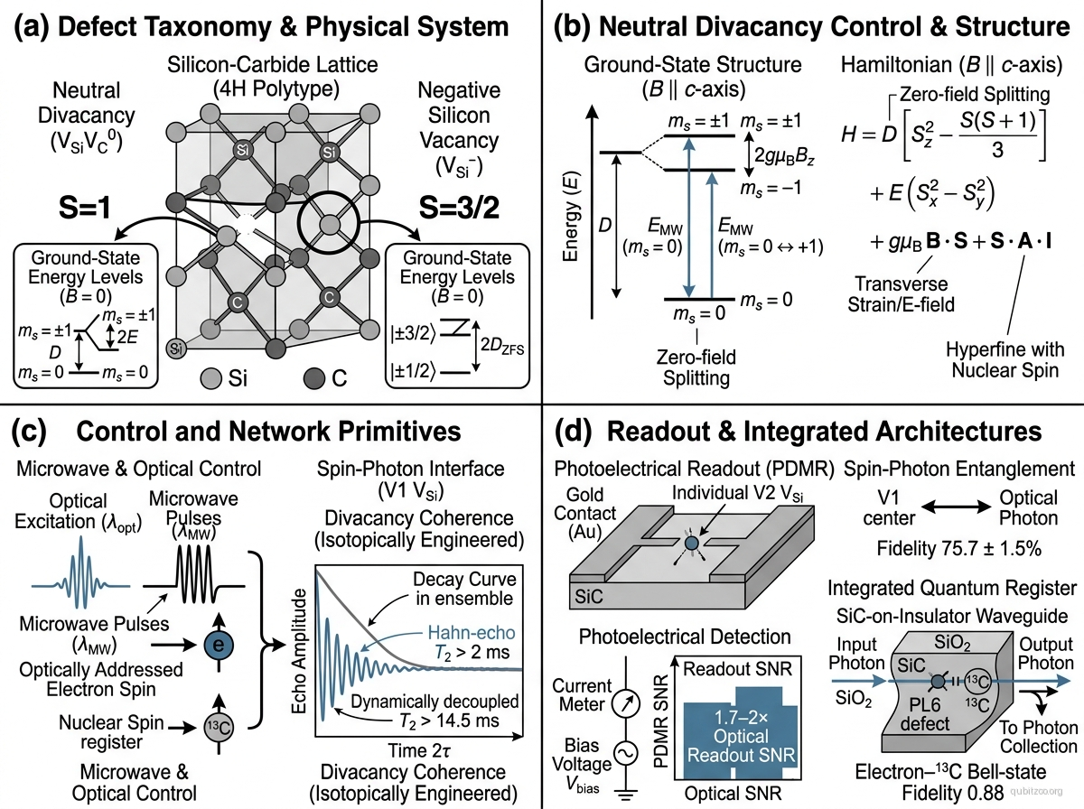
Description
Silicon-carbide defect qubits use optically addressable electron spins associated with point defects in a technologically mature wide-band-gap semiconductor. Two major branches must not be conflated: the neutral divacancy has an ground state analogous in control language to diamond NV centers, while the negatively charged silicon vacancy has an ground state and different level structure.
SiC combines optical initialization/readout, microwave spin control, nearby nuclear-spin registers, and wafer-scale growth and nanofabrication. Its near-infrared optical transitions are attractive for spin-photon interfaces, though spectral stability and photon collection remain less mature than the best diamond nanophotonics.
Hamiltonian
For an axial neutral divacancy, a useful ground-state spin Hamiltonian is
with , zero-field splitting , transverse strain/electric-field parameter , and hyperfine tensor . Both and the sign and magnitude of the optical spin contrast depend on polytype, lattice site, and defect configuration, so values such as GHz apply to a specified center (for example PL6), not to every SiC divacancy. Silicon-vacancy centers require an crystal-field Hamiltonian; they are a related defect branch, not the same qubit.
Motivation
- Retain optically addressable defect-spin physics in a semiconductor with established wafer processing.
- Integrate spin memories with nanophotonic cavities and electrical devices on the same material platform.
- Exploit multiple defect species and nuclear-spin registers while maintaining a clear physical taxonomy.
Experimental Status
Room-temperature coherent control of SiC defect spins was demonstrated in 2011. Christle et al. isolated and coherently controlled individual neutral divacancies and measured ensemble Hahn-echo coherence exceeding 1 ms. Nagy et al. demonstrated high-fidelity spin and optical control of single silicon-vacancy centers in 4H-SiC.
The platform has since advanced from isolated-spin control to network-node primitives. Bourassa et al. entangled a divacancy electron spin with a single Si nuclear spin while reporting 99.984(1)% electron-spin control fidelity and ms. Fang et al. generated V1 silicon-vacancy spin–photon entanglement with fidelity %. In 2024, Hu et al. prepared an ambient-condition PL6 electron–C Bell state with fidelity 0.89 and retained 0.88 after integration into a silicon-carbide-on-insulator waveguide. Nishikawa et al. then demonstrated coherent room-temperature photoelectrical readout of an individual V2 silicon-vacancy spin with 1.7–2 times the signal-to-noise ratio of their optical readout. Morioka et al. broadened the electrical-readout picture in 2026 by demonstrating coherent photoelectrical detection and spectroscopy of PL3 and PL5–PL7 ensembles.
Key Metrics
| Metric | Value | Notes | Fidelity reference |
|---|---|---|---|
| Hahn-echo | >1 ms | Neutral divacancy ensemble in high-purity 4H-SiC | Christle et al. 2015 |
| Electron-spin control | 99.984(1)% | Isotopically engineered divacancy; randomized benchmarking | Bourassa et al. 2020 |
| Dynamically decoupled | >14.5 ms | Isotopically engineered divacancy; Hahn echo ms | Bourassa et al. 2020 |
| Spin–photon entanglement fidelity | % | V1 silicon vacancy, time-bin photonic qubit | Fang et al. 2024 |
| Electron–nuclear Bell-state fidelity | 0.89 (0.88 after waveguide integration) | PL6 divacancy–C register at ambient conditions | Hu et al. 2024 |
| Operating regime | Room temperature demonstrated | Coherent defect-spin control | Koehl et al. 2011 |
| Single-spin photoelectrical readout | 1.7–2× optical-readout SNR | Individual V2 silicon vacancy at room temperature | Nishikawa et al. 2025 |
| Photoelectrical readout | Room-temperature coherent PDMR | PL3 and PL5–PL7 defects | Morioka et al. 2026 |
| Defect branches | and | Divacancy and silicon-vacancy encodings | Nagy et al. 2019 |
Scaling Considerations
- Different polytypes, lattice sites, and charge states create a rich but fragmented device landscape.
- Transform-limited optical lines and stable charge-state control are required for remote entanglement.
- Isotopic purification and nuclear-spin engineering can extend coherence but add materials complexity.
- Foundry compatibility is promising, but reproducible cavity-coupled single-defect yield remains a bottleneck.
- Photoelectrical magnetic-resonance readout offers a path around inefficient near-infrared photon collection, but defect-dependent ionization and electrical contrast still require device-level optimization.
References
- W. F. Koehl et al., “Room temperature coherent control of defect spin qubits in silicon carbide,” Nature 479, 84–87 (2011).
- D. J. Christle et al., “Isolated electron spins in silicon carbide with millisecond coherence times,” Nature Materials 14, 160–163 (2015).
- R. Nagy et al., “High-fidelity spin and optical control of single silicon-vacancy centres in silicon carbide,” Nature Communications 10, 1954 (2019).
- A. Bourassa et al., “Entanglement and control of single nuclear spins in isotopically engineered silicon carbide,” Nature Materials 19, 1319–1325 (2020); arXiv:2005.07602.
- R.-Z. Fang et al., “Experimental Generation of Spin-Photon Entanglement in Silicon Carbide,” Physical Review Letters 132, 160801 (2024); arXiv:2311.17455.
- H. Hu et al., “Room-temperature waveguide integrated quantum register in a semiconductor photonic platform,” Nature Communications 15, 10256 (2024).
- T. Nishikawa et al., “Coherent photoelectrical readout of single spins in silicon carbide at room temperature,” Nature Communications 16, 3405 (2025).
- N. Morioka et al., “Photoelectrical detection and characterization of divacancy and PL5–PL7 spins in silicon carbide,” Physical Review B 113, 104426 (2026); arXiv:2512.05283.
Linked Papers
- koehl-2011-sic-defect-spin-control
- christle-2015-sic-divacancy
- nagy-2019-sic-silicon-vacancy
- bourassa-2020-sic-nuclear-spin-register
- fang-2024-sic-spin-photon-entanglement
- hu-2024-sic-waveguide-quantum-register
- nishikawa-2025-sic-single-spin-photoelectrical-readout
- morioka-2026-sic-photoelectrical-readout
Evergreen context
- coherence-time-hierarchy — connects electron-spin operations to longer nuclear-memory timescales.
- divincenzo-criteria — evaluates the trade between local spin quality and network-interface maturity.
- spin-photon-interfaces-separate-emission-collection-and-wavelength-matching — identifies spectral stability and reproducible cavity/waveguide coupling as the interface bridge between SiC’s local register and a scalable network node.
Related Entries
- nv-center-qubit — diamond defect-spin baseline.
- siv-color-center-qubit — group-IV diamond defects optimized for optical quality.
- t-center-qubit — telecom-adjacent silicon defect node.
- quantum-transduction — frequency conversion for linking near-infrared SiC emitters to telecom networks.
- qubit-readout — optical and emerging photoelectrical spin-readout methods.