Figure
Description
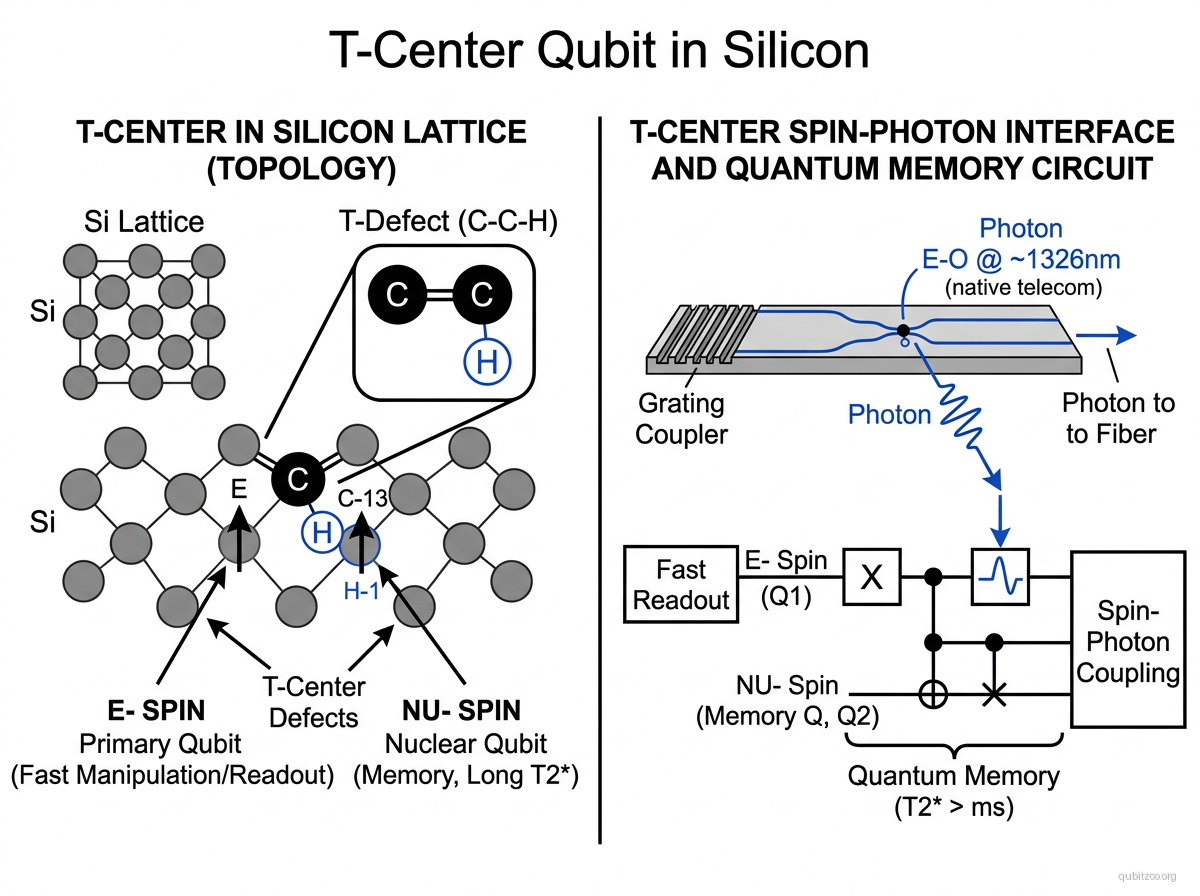
The silicon T centre is a telecom-band spin-photon interface built from a carbon-pair plus hydrogen defect complex in silicon, commonly modeled as a C-C-H complex. Its optical zero-phonon line sits near 1326 nm in the telecom O-band, so it can interface directly with standard fibre components without the frequency conversion usually needed for visible-wavelength solid-state emitters.
A single T centre combines an optically addressable electron spin with nearby nuclear-spin memories. Depending on isotopic configuration, the register can include the electron spin, the hydrogen nuclear spin, and up to two nearby ¹³C nuclear spins. That combination makes the platform interesting not just as a photon source, but as a small local memory-and-processing node inside a silicon photonics stack.
Experimentally, the platform has moved in distinct steps. Bergeron et al. (2020) established the integrated telecom photon-spin interface in silicon. Higginbottom et al. (2022) reported optical observation of single spins in silicon T centres. DeAbreu et al. (2023) demonstrated waveguide-integrated T centres. A 2024 Photonic Inc. preprint then reported remote entanglement between T centres in separate cryostats and a preliminary, post-selected teleported CNOT sequence over a selected basis set. In 2025, electrically triggered spin-photon devices in silicon showed that T-centre nanophotonics can also be driven electrically, not only optically.
Hamiltonian
A representative ground-state spin Hamiltonian is
where is the electron spin, are the coupled nuclear spins (¹H and, when present, ¹³C), is the electron tensor, and are hyperfine tensors. For an encyclopedia entry this captures the essential physics: a Zeeman-split electron spin coupled to one or more long-lived nuclear memories.
The optical interface is mediated by a bound-exciton manifold with transition energy near the telecom O-band zero-phonon line. A minimal driven model is
with THz (1326 nm). In real devices, orientation-dependent selection rules, excited-state structure, and spectral diffusion matter for entanglement generation and readout.
Motivation
- Telecom-native: The 1326 nm transition is already in the telecom O-band, easing fibre networking and chip-to-chip photonic interconnects.
- Silicon-native: The platform lives inside silicon and can leverage mature silicon photonics and semiconductor processing.
- Small local register: One defect can host an optically active electron spin plus nuclear-spin memory qubits.
- Modular architecture fit: Heralded remote entanglement offers a natural path to non-local interconnects between cryogenic modules.
- Networking first, then computation: T centres are especially compelling where communication, memory, and distributed gates matter simultaneously.
Experimental Status
Integrated telecom spin-photon interface — Bergeron et al. (2020):
- Established the silicon-integrated telecom photon-spin interface
- Optical transition near 1326 nm in the telecom O-band
- Electron-spin coherence on the millisecond scale in isotopically enriched ²⁸Si
Single-spin optical observation — Higginbottom et al. (2022):
- Optical observation of individual T-centre spins in silicon
- Cavity-coupled nanophotonic devices with single-spin readout capability
Waveguide integration — DeAbreu et al. (2023):
- Waveguide-integrated silicon T centres demonstrated
- Strengthened the case for scalable on-chip routing and collection
Distributed quantum computing proof-of-concept — Photonic Inc. (2024 preprint):
- Remote Bell-pair generation between T centres in separate cryostats connected by telecom fibre
- Measured Bell-pair fidelity reached 0.60(0.08) at a 40 ns time-bin width
- Reported a preliminary, post-selected teleported CNOT truth table over a selected basis set, rather than a full deterministic remote gate benchmark
Electrical triggering — Dobinson et al. (2025):
- Electrically triggered silicon spin-photon devices demonstrated
- Included electrically driven O-band emission and electrically generated single-photon / spin-photon functionality in T-centre nanophotonics
Key Metrics
| Metric | Value | Notes | Fidelity reference |
|---|---|---|---|
| Emission wavelength | 1326 nm | Telecom O-band zero-phonon line | Bergeron et al. 2020 |
| Electron spin T₂ | ~2 ms | Reported in isotopically enriched ²⁸Si | Bergeron et al. 2020 |
| Nuclear-spin memory | >1 s | Long-lived local memory register | Bergeron et al. 2020 |
| Remote Bell-pair fidelity | 0.60(0.08) | 40 ns time-bin width, preliminary 2024 preprint | Photonic Inc. 2024 |
| Teleported gate sequence | Demonstrated | Post-selected preliminary tCNOT truth table over a selected basis set | Photonic Inc. 2024 |
| Electrical triggering | Demonstrated | Electrically driven T-centre spin-photon devices in silicon | Dobinson et al. 2025 |
Scaling Considerations
- Silicon photonics compatibility: Waveguide and cavity integration are real experimental milestones, not just a platform promise.
- Telecom networking advantage: Native O-band emission removes a major systems burden that many other solid-state spin-photon platforms carry.
- Distributed-computing relevance: The platform has already crossed from isolated emitter physics into remote-entanglement experiments, albeit still at proof-of-concept scale.
- Architectural caveat: Claims about qLDPC-friendly non-local connectivity are best viewed as architectural motivation, not yet as an experimentally validated fault-tolerant stack.
- Device roadmap: Electrical triggering is an important maturity step because it points toward more integrated cryogenic photonic hardware.
References
Foundational interface and control milestones
- L. Bergeron et al., “Silicon-Integrated Telecommunications Photon-Spin Interface,” PRX Quantum 1, 020301 (2020)
- D. B. Higginbottom et al., “Optical observation of single spins in silicon,” Nature 607, 266-270 (2022)
- A. DeAbreu et al., “Waveguide-integrated silicon T centres,” Optics Express 31, 15045-15057 (2023)
Distributed and device-integration milestones
- Photonic Inc., “Distributed Quantum Computing in Silicon” (2024 preprint) — remote Bell-pair generation and a preliminary post-selected teleported-gate sequence, arXiv:2406.01704
- M. Dobinson et al., “Electrically triggered spin-photon devices in silicon,” Nature Photonics (2025)
Linked Papers
- bergeron-2020-silicon-integrated-telecommunications
- higginbottom-2022-optical-observation-of-single-spins-in-silicon
- deabreu-2023-waveguide-integrated-silicon-t-centres
- photonic-2024-distributed-qc
- dobinson-2025-electrically-triggered-spin-photon-devices-in-silicon
Evergreen context
- divincenzo-criteria — T centres are notable because the same silicon defect platform addresses stationary-spin storage and optical communication, rather than bolting a separate transducer onto an otherwise disconnected qubit.
- coherence-time-hierarchy — the platform naturally fits a layered-memory picture: an optically active electron spin for interfacing, plus slower but much longer-lived local nuclear-spin storage.
Related Entries
- nv-center-qubit — diamond color center benchmark for spin-photon networking, but visible-wavelength rather than telecom-native
- siv-color-center-qubit — strong optical diamond color-center family with different coherence and wavelength tradeoffs
- silicon-spin-qubit — silicon spin hardware without the native telecom optical interface
- quantum-transduction — contrast case where frequency conversion is needed because the emitter is not already in the telecom band
- qldpc-codes — architectural context for why non-local interconnects are attractive
- dual-rail-photonic-qubit — photonic flying-qubit layer that can interface with remote entanglement protocols