Figure
Description
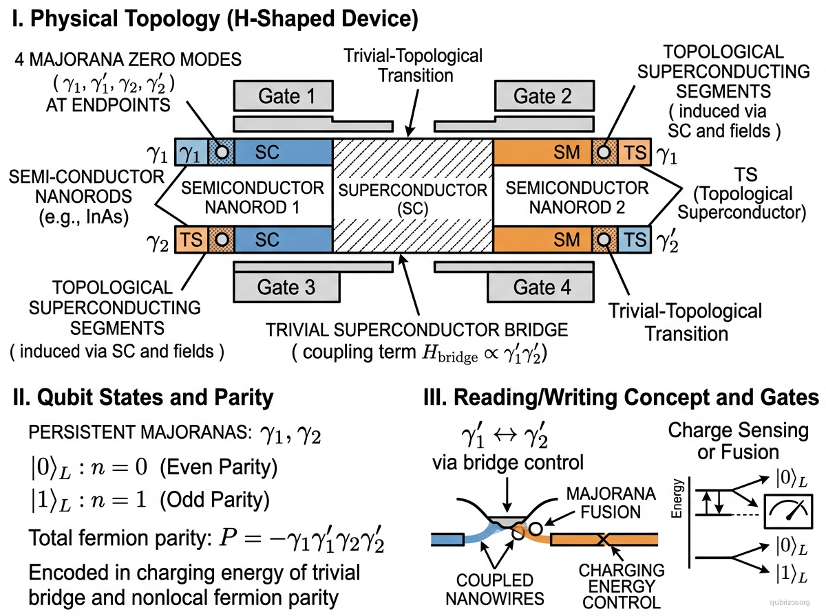
The tetron is a topological qubit design encoding quantum information in the joint fermion parity of four Majorana zero modes (MZMs) arranged in an H-shaped semiconductor-superconductor heterostructure. The qubit states and correspond to even and odd total parity of MZM pairs, and are topologically protected against local perturbations. The tetron is the architecture behind Microsoft’s Majorana 1 processor (2025).
Four MZMs are hosted at the endpoints of two parallel topological superconductor segments connected by a trivial superconducting bridge (forming an “H” shape). The logical qubit is encoded in the parity degree of freedom:
where is the fermion parity of MZM pair .
Gate operations use measurement-based braiding: joint parity measurements of MZM pairs implement effective braiding without physically moving quasiparticles. Parity readout uses quantum dot sensors coupled to MZM pairs via charge sensing. The complete Clifford group is achieved from single-qubit parity measurements plus two-qubit joint measurements.
Microsoft’s 2025 Majorana 1 processor implements 8 tetron qubits using InAs/Al heterostructures (“topoconductors”). Key claims include topological gap protocol passed, controlled MZM parity, and a path toward 4×2 arrays with entanglement, targeting ~10× reduction in QEC overhead compared to conventional superconducting qubits.
Hamiltonian
Low-energy effective Hamiltonian for four MZMs:
where are Majorana operators (, ) and are exponentially suppressed overlap energies. Topological protection: where is the separation and the coherence length.
Motivation
- Topological protection: Qubit states are protected by topology — local perturbations cannot distinguish from , giving exponentially suppressed error rates.
- Measurement-only gates: No physical braiding needed — simplifies device layout and eliminates braiding-speed limitations.
- QEC overhead reduction: Microsoft claims ~10× fewer physical qubits needed for fault-tolerant computation vs. transmon + surface code.
- Scalable architecture: H-shaped design is lithographically defined and compatible with semiconductor fabrication; 4×2 arrays are near-term targets.
Evergreen context
- quantum-hardware situates the tetron as an architecture-layer proposal, not a new materials platform by itself: it packages Majorana physics into a qubit-and-array design.
- divincenzo-criteria clarifies the real bottlenecks, namely parity initialization, repeated high-fidelity measurement, and controlled two-qubit operations under quasiparticle-poisoning constraints.
- threshold-theorem is the right lens for Microsoft’s overhead claims, because a 10× savings matters only if the protected physical error model really moves the architecture deeper below fault-tolerance threshold.
- spin-orbit-coupling-for-qubit-control remains upstream of the whole design, since the InAs/Al heterostructures rely on strong spin-orbit-coupled semiconductor physics to enter the topological regime in the first place.
Key Metrics
| Metric | Value | Notes | Fidelity reference |
|---|---|---|---|
| Topological gap | ~20–40 μeV | InAs/Al topoconductor | Aghaee et al. 2025 |
| MZM count | 4 per tetron | H-shaped device | Karzig et al. 2017 |
| Parity lifetime | TBD | Key open metric | — |
| QEC overhead reduction | ~10× claimed | vs. transmon surface code | Aghaee et al. 2025 |
Scaling Considerations
- Measurement-only topological QC: No physical braiding needed — simplifies device layout.
- Modular arrays: 4×2 tetron arrays planned as building blocks for larger processors.
- QEC synergy: Topological protection at physical level reduces logical overhead.
- Materials challenge: Requires pristine semiconductor-superconductor interfaces with hard induced gap.
References
Original proposal
- T. Karzig et al., “Scalable designs for quasiparticle-poisoning-protected topological quantum computation with Majorana zero modes,” Phys. Rev. B 95, 235305 (2017) — arXiv:1610.05289
Experimental progress
- M. Aghaee et al. (Microsoft Quantum), “Interferometric single-shot parity measurement in an InAs-Al hybrid device,” Nature 638, 651 (2025) — arXiv:2405.10269
Linked Papers
Related Entries
- majorana-topological-qubit — General Majorana qubit concept
- planar-josephson-junction-qubit — Related InAs/Al heterostructure physics
- surface-code-logical-qubit — Conventional QEC approach that tetrons aim to improve upon